The only other thing I can think of is some purpose like HFT may need to fit a whole algorithm in L3 for absolute minimum latency, and maybe they want only the best core in each chiplet? It's probably about software licenses, though.
And like you say, plenty of times it is infeasible to rewrite the code because its third party code for which you don't have the source or the rights.
A couple years ago I noticed that some Xeons I was using had a much cache as the ram in the systems I had growing up (millennial, so, we’re not talking about ancient commodores or whatever; real usable computers that could play Quake and everything).
But 512MB? That’s roomy. Could Puppy Linux just be held entirely in L3 cache?
Zen 4 also had 96 MB per CCD variants like the 9184X, so 768 MB per, and they are dual socket so you can end up with a 1.5 GB of total L3 cache single machine! The downside being now beyond CCD<->CCD latencies you have socket<->socket latencies.
Though I wish they did some chips with 128GB of high bandwidth dram instead of a extra sized sram caches.
> The RAMpage memory hierarchy is an alternative to a conventional cache-based hierarchy, in which the lowest-level cache is managed as a paged memory, and DRAM becomes a paging device.
https://www.mathworks.com/products/matlab-parallel-server/li....
It’s common practice to test algorithms with different numbers of threads and then use the optimal number of threads. For memory-intensive algorithms the peak performance frequently comes in at a relatively small number of cores.
I worked on high perf around 10 years ago and at that point I would pin the OS and interrupt handling to a specific core so I’d always lose one core. Testing led me to disable hyperthreading in our particular use case, so that was “cores” (really threads) halfed.
A colleague had a nifty trick built on top of solarflare zero copy but at that time it required fairly intrusive kernel changes, which never totally sat well with me, but again I’d lose a 2nd core to some bookkeeping code that orchestrated that.
I’d then tasksel the app to the other cores.
NUMA was a thing by then so it really wasn’t straightforward to eek maximum performance. It became somewhat of a competition to see who could get highest throughout but usually those configurations were unusable due to unacceptable p99 latencies.
* Ampere MSRP $5.5K vs $15K for the EPYC.
* Turin 196 had 1.6x better performance
* Ampere had 1.2x better energy consumption
In terms of actual $/perf, Ampere 192 core is 1.7x better than Turin Dense 196 core based on Phoronix's review.
So for $5.5k, you can either buy an AmpereOne 192 core CPU (274w) or a Turin Dense 48 core CPU (300w).
Ampere has a 256 core, 3nm, 12 memory channel shipping next year that is likely to better challenge Turin Dense and Sierra Forest in terms of raw performance. For now, their value proposition is $/perf.
Anyway, I'm very interested in how Qualcomm's Nuvia-based server chips will perform. Also, if ARM's client core improvements are any indication, I will be very interested in how in-house chips like AWS Graviton, Google Axion, Microsoft Cobalt, Nvidia Grace, Alibaba Yitian will compete with better Neoverse cores. Nuvia vs ARM vs AmpereOne.
This is probably the golden age of server CPUs. 7 years ago, it was only Intel's Xeon. Now you have numerous options.
You're comparing it to the highest MSRP Turin, which doesn't have the highest performance/$. People buy that one if they want to maximize density or performance/watt, where it bests Ampere. If you only care about performance/$ you would look at the lower core count Zen5 (rather than Zen5c) models which have twice the performance/$ of the 192-core 9965.
Doing the same for Ampere doesn't work because their 192-core 3.2GHz model is very nearly already their peak performance/$.
Twenty years ago we had just 1-2 cores per CPU, so we were lucky to have 4 cores in a dual socket server.
A single server can now have almost 400 cores. Yes, we can have even more ARM cores but they don't perform as well as these do, at least for now.
800Gbps from a single server was achieved by Netflix on much lesser systems two years ago:
https://nabstreamingsummit.com/wp-content/uploads/2022/05/20...
If I were to guess, this hardware can do double that, also helping that we now have actual 800Gbps Ethernet hardware.
Indeed 20 years ago this would have been racks of gear at a very high cost and a huge power bill.
Or if our medium point is a 60 watt pentium 4 then our final point would be a 1200 watt single core with multiple millions of times the performance, and dropping down to 300 watts would still be crazy fast.
That said, sometimes The Cloud goes down too.
Individual tasks would definitely have better latency, but I'd suspect the impact on throughput/CPU usage might be muted. Of course at the extremes (very small jobs, very large/complex objects being passed) you'd see big gains.
I suspect you would be able to cut down the 2.5hr runtime dramatically even with the Spark if you just deployed it as a single instance on that very same 32vCPU machine.
I'm not against using simple methods where appropriate. 95% of the companies out there probably do not need frameworks like spark. I think the main argument against them is operational complexity though, not the compute overhead.
Imagine an example where you have two arrays of 1 billion numbers, and you want to add them pairwise. You could use spark to do that by having each "task" be a single addition. But the time it would take to structure and transmit the 1 billion requests will be many multiples of the amount of time it would take to just do the additions.
[1] https://www.cpushack.com/2014/08/25/national-semiconductor-c...
To quote the announcement: "two VLIW (very long instruction word) microprocessors on a single piece of silicon"
> Sun built a single model of the MAJC, the two-core MAJC 5200, which was the heart of Sun's XVR-1000 and XVR-4000 workstation graphics boards.
Why have I not heard of those before?
Also not worth getting anything less than 3rd gen unless you're primarily buying them for the pcie lanes and ram capacity - a regular current gen consumer CPU with half - a quarter of the core count will outperform them in compute while consuming significantly less power.
https://www.servethehome.com/amd-psb-vendor-locks-epyc-cpus-...
Doing that on Intel platforms just wasn't done for basically ever, it was never worth it. But upgrade to Milan from Naples or Rome is very appealing.
So SP3 CPUs are much more common used than the boards, simply because more of them were made. This is probably very bad for hobbyists, the boards are not going to get cheap until the entire platform is obsolete.
However when you end up building a server quite often the motherboard + case is the cheap stuff, the CPUs are second in cost and the biggest expense can be the RAM.
I snagged a 9 5950X for £242
With the loss of Anandtech, TechReport, HardCOP and other old technical sites, I'm glad to see a new publisher who can keep up with the older style stuff.
At least for now.
[1] https://www.amd.com/en/products/processors/server/epyc/9005-...
Inter-core latency will be rough since you'll always be hitting the relatively slow inter-chiplet bus, though.
> AMD has ported early AGESA features to the PSP, which now discovers, enables and trains DRAM. Unlike any other x86 device in coreboot, a Picasso system has DRAM online prior to the first instruction fetch.
Perhaps they saw badly trained RAM as a security flaw? Or maybe doing it with the coprocessor helped them distribute the training code more easily (I heard a rumour once that RAM training algos are heavily patented? Might have imagined it).
Using it as TCM ram seems super useful.
Although you would need to fight/request it from the OS, so technically I see why they might ditch it.
It would never flush any cache lines to RAM, and never do any reads from RAM.
Is this all ECC memory at these speeds?
https://www.amd.com/en/products/processors/server/epyc/9005-...
It has 16 CCD, each with only one thread enabled, latency between CCD is ~150ns.
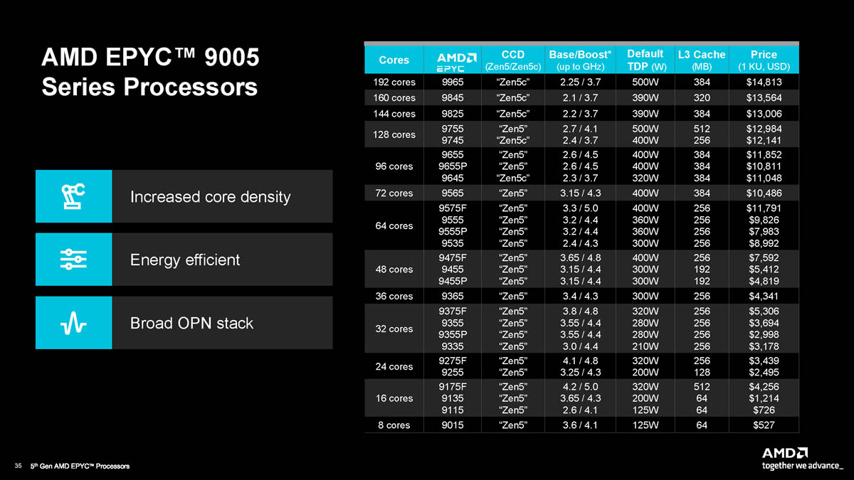
Has the full range with TDP. 500w is only for the 128/192 monster chips. The 16 core fast sku has a 320W TDP.
That being said, it looks most probable what a 9175F is just a 9755 (their absolute max full size Zen5 core part) with nearly all (7/8) of their cores per CCD disabled in order to get all 512MB of cache. This means that there's a lot of extra interconnect being kept running per core which certainly would contribute to the higher TDP.
Of course, in principle this should also mean that each core (which should basically have all of a CDD's IO and cache available to it) should be screaming fast in real terms.
Of course finally, TDP is a totally fluffy number. The TDP of the 7950X3D is most probably as low as it is because of how much internal thermal resistance (the extra V-Cache layer) it has. Part of it's lower TDP isn't because "it's efficient", part of it is because "if we run it hotter, we'll melt it". The TDP for the 7950X for example is 170W.
Socket sp5 is more than 3x the area of am5.
With recent DDR generations and many core CPUs, perhaps CPUs will give GPUs a run for their money.
Since it takes 4 cycles to execute FMA on double-precision 64-bit floats (VFMADD132PD) this translates to 1.25G ops/s (GFLOPS/s) per each core@5GHz. At 192 cores this is 240 GFLOPS/s. For a single FMA unit. At 2x FMA units per core this becomes 480 GFLOPS/s.
For 16-bit operations this becomes 1920 GFLOPS/s or 1.92 TFLOPS/s for FMA workloads.
Similarly, 16-bit FADD workloads are able to sustain more at 2550 GFLOPS/s or 2.55 TFLOPS/s since the FADD is a bit cheaper (3 cycles).
This means that for combined half-precision FADD+FMA workloads zen5 at 192 cores should be able to sustain ~4.5 TFLOPS/s.
Nvidia H100 OTOH per wikipedia entries, if correct, can sustain 50-65 TFLOP/s at single-precision and 750-1000 TFLOPS/s at half-precision. Quite a difference.
For a Zen 5 core, that means 16 double precision FMAs per cycle using AVX 512, so 80gflop per core at 5ghz, or twice that using fp32
This is actually a bit crazy when you stop and think about it. Nowadays CPUs are packing more and more cores per die at somewhat increasing clock frequencies so they are actually coming quite close to the GPUs.
I mean, top of the line Nvidia H100 can sustain ~30 to ~60 TFLOPS whereas Zen 5 with 192 cores can do only half as much, ~15 to ~30 TFLOPS. This is not even a 10x difference.
Where the balance slants all the way towards gpus again is the tensor units using reduced precision...
Admittedly I also have no idea why Intel calls theirs Xeon, which sounds like misspelled xenon. But then it might be a proper Greek word?
The criticism above says "Turin, Epyc and lord knows what else". That clearly includes the codenames.
The marketing departments of monitor manufacturers still haven't figured this one out yet.
> Looks like the folks downvoting me are massive, massive fans of that THREADRIPPER architecture.
Yes, it must be everybody else, not your comment, which is the pinnacle of deep analysis. Get real, dude.
Compare with List of AMD processors[2] and a "70xx" model could be a Zen Naples Epic, A Zen 2 Mendocino Ryzen, a Zen 2 Rome Epyc, a Barceló-R Ryzen Zen 3, a Milan Epyc Zen 3, a Rembrandt-R Zen 3+, a Zen 4 Raphael Ryzen or Storm Peak Threadripper, or a laptop Ryzen. Wikipedia people can't even put these into a table to compare them, it's pages of random names and overlapping/re-used numbers.
Apple, as usual, have M1, M2, M3 and each one has plain/pro/max/ultra.
[1] https://en.wikipedia.org/wiki/List_of_Intel_processors#Lates...
Well no, the comparison to "Epyc" is "Intel Core" and "Ryzen"
And if you gave each SKU its own name I think that would very quickly get worse than the stupid numbering schemes.
64 cores is a high-end gaming rig. Civilization VII won't run smoothly on less than 16.
https://i.imgur.com/YlJFu4s.png
Whether the bottleneck is memory bandwidth (2x6000 MHz), unoptimized locking, small batch sizes, or something else it doesn't seem to be related to core count. It's also not waiting on the GPU much here, the 4090 is seeing even less utilization than the CPU. Hopefully utilization actually scales better with 7, not just splits up a lot.
As a rule I wouldn't be surprised if 90% of the stuff Civ 6 is doing can't be parallelized at all, but then for that remaining 10% you get a 16x speedup with 16 cores. And they're underutilized on average but there are bursts where you get a measurable speedup from having 16 cores, and that speedup is strictly linear with the number of cores. 6 cores means that remaining 10% will be less than half as fast vs. having 16 cores. And this is consistent with observing 30% CPU usage I think.
Why do you type it like that?
It's weird/juvenile to be typing a phrase in a manner similar to a preteen, well after 20+ years have passed. Especially in the middle of an otherwise normal message/conversation.
Though I think this guy just did it the way a 2000s kid would say "vidya gaems".
A surprising number of video games have at least one 'master switch' statement for at least one important aspect of the game logic that has to evaluate on a single thread to maintain some level of 'coherency' while operating at any given frame rate.
The challenge with using threads without careful control of or understanding of the underlying system hardware is that you can wind up with various quirks (Every computer I had from 2000-2010 had this weird 'judder' with HL/TFC/HL2 and explosions, didn't matter the sound card type, CPU brand, or Video card brand,) at best or a rats nest of logic bugs at worst (i.e. the pains of coding multithreading.)
Only recently I managed to build a PC that will run Civ 6 smoothly during late game on huge map
Tangentially related, but I need to go check a18 civ 6benchmarks. The experience on my a15 with small map sizes was surprisingly good.
[1] Fragmentation, at best C++ dialects, no practical compiler tech to transparently GPU offload, etc